|
|
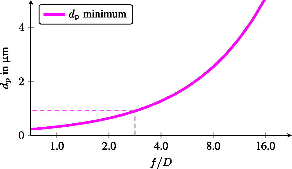
1.IntroductionThe steady progress in semiconductor technology allows the manufacturing of smaller and smaller structures and image sensors with ever shrinking pixel sizes. One can get the impression that the pixel size is just limited by the technology and even smaller pixels are desirable. Today, consumer products with pixel sizes are already on the market and devices with are in production.1 In comparison, photo receptors in the human eye are reported to be larger than 3 μm.2 The general modeling of light is well understood,3 and simulation with commercial tools like ISET4 is possible. In contrast, this letter addresses parameters like aperture and pixel size and their photometric consequences for modeling the amount of light that is available in a digital video camera system. One of the design parameters is the resulting image quality. With small pixels only a few photons will hit a single pixel during an exposure period and the signal-to-noise power ratio (SNR) will be poor due to shot noise.5 Apart from all technological limitations, this physical boundary limits the performance of today’s video cameras. 2.Image Acquisition ModelThe scene radiates a certain amount of light. This is described by an average radiance in object space . The sensor sees an effective amount of light equivalent to the cone with a solid angle as shown in Fig. 1(a). This cone is defined by the sphere of radius equal to the focal length and a circular aperture disk with diameter . The solid angle thus calculates to6 The sensor receives an irradiance for a lens with optical transmittance .Fig. 1Parameters of (a) focal length , aperture diameter and resulting solid angle and (b) quadratic pixels with fill factor . 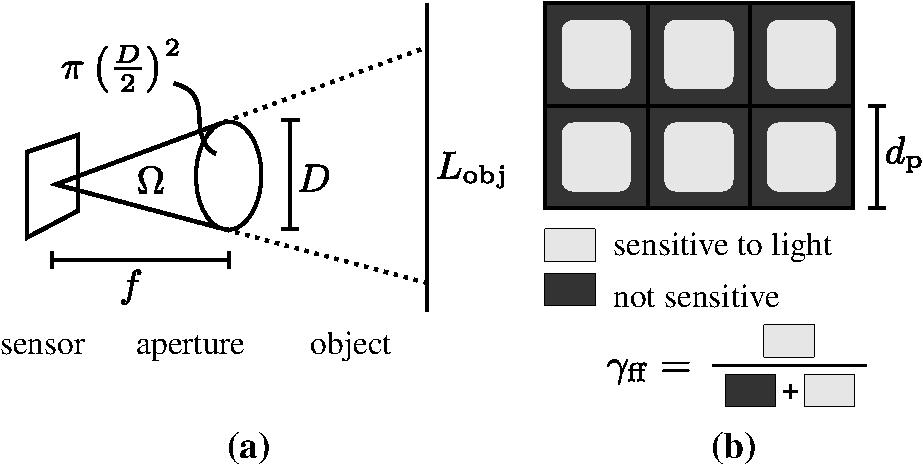 On the sensor some area is used for interconnects and transistors so that only some of the area is sensitive to light. Figure 1(b) shows pixels of size . The ratio of active to total areas is expressed as an effective sensor fill factor . Even with clever manufacturing like micro-lenses or back side illumination, holds. A single pixel thus captures a certain amount of radiant power (radiant flux) of the sensor irradiance A single photon of wavelength has the energy with the speed of light and Planck’s constant . The radiant flux thus consists of photons during a certain time interval (exposure time) of . In the photoreceptor only some of these photons are converted into electrons while others are not, due to reflection, recombination and other material interactions. The conversion rate is expressed as quantum efficiency .7 The electrons are then collected in the pixel. Although we will see , on average, the charge is still quantized and the actual number of electrons is subject to shot noise due to the occurrence of random events. For electrons the associated shot noise is of strength .5 As , signal power is represented with and SNR thus calculates to In CCD or CMOS technology there are further sources of sensor noise,8 which are neglected in the ideal case.SNR is a parameter that is directly visible in the final images. For answering the original question, we can combine the above equations. This leads to 3.Results for Ideal SystemAt first we assume ideal technology. A typical indoor scene is illuminated with a luminance of .9 For the peak sensitivity of the human eye at a wavelength of the SI unit candela is defined10 as radiant intensity of . The radiance in object space is then We further assume a perfectly transparent lens with , a wide aperture , fill factor and quantum efficiency . For achieving typical video frame rates a maximum exposure time of is used. For a human observer, images without visible noise are preferred. From psychophysical studies a thousand-photon limit is reported as the threshold for visibility of shot noise.5 We therefore set . With green light with the minimum pixel size calculates to .The influence of different apertures is shown in Fig. 2. With larger aperture diameters, even smaller pixels can be used. A variation of luminance is also possible: In practice, the human color perception (photoptic vision) starts at .9 The luminance in daylight exterior scenarios is typically .9 The resulting minimum pixel sizes thus range from 5 to 0.09 μm as shown in Fig. 3. 4.Radiometric ModelingUp to now, we used monochromatic light only. We now extend this and also include the spectral distribution of light. Again, we start with a scene with a luminance of . Now, the light is made up of radiation from a light bulb. This is modeled as a black body at a certain color temperature and a spectral radiance of With the photoptic luminous efficiency function11 , we set with . The resulting normalized spectral radiance is now perceived by the human eye as a luminance of . Figure 4 shows the resulting set of normalized spectral radiances for typical color temperatures.Fig. 4Spectral radiance of black bodies with temperatures , intensity scaled to be perceived as luminance of . 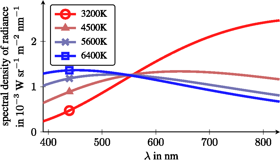 Today, most cameras are used to capture scenes for later viewing by a human. The camera should therefore create a representation of the scene that is similar to that of the human visual system. We simulate an ideal camera with the spectral sensitivity curves based on the Stockman and Sharpe cone measurements of the human eye.12 The corresponding spectral sensitivity functions for long (L), medium (M) and short (S) wavelengths are shown in Fig. 5. However, we assume an ideal camera with ideal color filters and material without any attenuation () at peak efficiency. Fig. 5Sensitivity functions of 10-deg cone fundamentals for , and cone and luminous efficiency function .  In Table 1, the resulting minimum pixel sizes are shown for the radiometric simulation. The luminosity case with monochromatic light at corresponds to the ideal simulation from above. There is less than 10% error for the simulation with and cones compared to the luminosity. This is plausible from the high similarity of the respective sensitivity curves. However, the capturing of blue light (short wavelengths with cone ) requires larger pixels. At short wavelengths, the individual photons have a higher energy and thus, there are fewer for a given radiant flux. This explains the problem of inferior performance of blue color channels in typical digital cameras. The extreme case of observing monochromatic green light with a short wavelength sensitivity leads to even fewer photons and would require pixels with 26 μm. In general, the monochromatic calculation is only slightly optimistic but gives a good approximation to a radiometric computation. Table 1Minimum pixel sizes (in μm) based on radiometric calculations for light sources with black body radiation of temperature T and monochromatic light source.
5.Results with Current TechnologyThe above numbers represent the theoretical limit for ideal sensors. In practice, a real world camera does not achieve these numbers. For example, a highly optimized three layer stacked image sensor is reported by Hannebauer et al.13 For pixels of size a high fill factor of and quantum efficiency of is possible with many (costly) optimizations. In current 1.4 μm consumer grade sensors the backside illumination (BSI) technology enables close to 100% fill factor.14 For color imaging, the spectral sensitivity is not without attenuation and peak quantum efficiencies of about are reported by OmniVision14 and Aptina.15 In scientific CMOS sensors, the combined sensor readout noise is reported as low as 16 and can thus be neglected among 1000 electrons. The combined assumption of , and leads to a minimum pixel size of . With mass-market sensors and additional noise,8 larger pixels are required. These small pixels also reach another technological limit of decreasing full well capacity. For example Aptina reports15 electrons, which leaves only a dynamic range of from noise visibility5 to overexposure. As a result, most of the image will still look noisy. However, this is a technological challenge that could be addressed with multiple readouts during the exposure.17 Another limitation comes with optical diffraction. Even in ideal optics the achievable resolution of a camera system is limited. The Sparrow criterion suggests3 that there is no gain in resolution below a critical pixel size of . For our example of and , we obtain . Achieving this limit, however, is challenging, especially in the off-axis field, and leads to expensive optics. A further decrease in aperture requires a dramatic increase of the technological efforts and smaller tolerances for optics manufacturers. 6.ConclusionIn our photometric analysis, we discuss the number of photons per pixel. With small pixels the image quality is limited by shot noise, and for indoor scenarios the current video cameras are surprisingly close to this fundamental limit. We estimate that even with ideal technology, a pixel size below will not capture enough light to generate visually pleasing videos any more. Current technology is far from perfect and with optimistic assumptions, the limit at is close to current sensors. However, for other imaging scenarios like outdoor daylight still photography, there is plenty of room at the bottom. ReferencesR. Fontaine,
“A review of the 1.4 um pixel generation,”
in Int. Image Sensor Workshop (IISW),
(2011). Google Scholar
J. B. JonasU. SchneiderG. O. H. Naumann,
“Count and density of human retinal photoreceptors,”
Graefes Arch. Clin. Exp. Ophthalmol., 230 505
–510
(1992). http://dx.doi.org/10.1007/BF00181769 GACODL 0721-832X Google Scholar
J. Goodman, Introduction to Fourier Optics, Roberts & Company Publishers, Englewood, Colorado, USA
(2005). Google Scholar
J. Farrellet al.,
“A simulation tool for evaluating digital camera image quality,”
SPIE Electron. Imag.—Image Quality and System Performance, 5294 124
–131
(2004). http://dx.doi.org/10.1117/12.537474 Google Scholar
F. XiaoJ. FarrellB. Wandell,
“Psychophysical thresholds and digital camera sensitivity: the thousand photon limit,”
SPIE Electron. Imag.—Digital Photography, 5678 75
–84
(2005). http://dx.doi.org/10.1117/12.587468 Google Scholar
R. Kingslake, Optical System Design, 1 Academic Press, London
(1983). Google Scholar
B. Fowleret al.,
“A method for estimating quantum efficiency for CMOS image sensors,”
SPIE Electron. Imag.—Solid State Sensor Arrays: Development and Applications II, 3301 178
–185
(1998). http://dx.doi.org/10.1117/12.304561 Google Scholar
R. Gowet al.,
“A comprehensive tool for modeling CMOS image-sensor-noise performance,”
IEEE Trans. Electron. Devices, 54 1321
–1329
(2007). http://dx.doi.org/10.1109/TED.2007.896718 IETDAI 0018-9383 Google Scholar
W. Smith, Modern Optical Engineering: The Design of Optical Systems, Tata McGraw-Hill Education, Englewood, Colorado, USA
(1990). Google Scholar
P. Giacomo,
“News from the BIPM: resolution 3—definition of the candela,”
Metrologia, 16
(1), 55
–61
(1980). http://dx.doi.org/10.1088/0026-1394/16/1/008 MTRGAU 0026-1394 Google Scholar
L. Sharpeet al.,
“A luminous efficiency function, , for daylight adaptation,”
J. Vision, 5
(11), 948
–968
(2005). http://dx.doi.org/10.1167/5.11.3 1534-7362 Google Scholar
A. StockmanL. Sharpe,
“The spectral sensitivities of the middle-and long-wavelength-sensitive cones derived from measurements in observers of known genotype,”
Vis. Res., 40
(13), 1711
–1737
(2000). http://dx.doi.org/10.1016/S0042-6989(00)00021-3 VISRAM 0042-6989 Google Scholar
R. Hannebaueret al.,
“Optimizing quantum efficiency in a stacked CMOS sensor,”
SPIE Electron. Imag.—Sensors, Cameras, and Systems for Industrial, Scientific, and Consumer Applications XII, 7875
(1), 787505
(2011). http://dx.doi.org/10.1117/12.873610 Google Scholar
H. Rhodeset al.,
“The mass production of second generation 65 nm BSI CMOS image sensors,”
in Int. Image Sensor Workshop (IISW),
(2011). Google Scholar
G. Agranovet al.,
“Pixel continues to shrink … pixel development for novel CMOS image sensors: a review of the 1.4 um pixel generation,”
in Int. Image Sensor Workshop (IISW),
(2011). Google Scholar
B. Fowleret al.,
“A 5.5 mpixel wide dynamic range low noise CMOS image sensor for scientific applications,”
SPIE Electron. Imag.—Sensors, Cameras, and Systems for Industrial/Scientific Applications XI, 7536 753607
(2010). http://dx.doi.org/10.1117/12.846975 Google Scholar
M. Schöberlet al.,
“Digital neutral density filter for moving picture cameras,”
SPIE Electron. Imag.—Computational Imag. VIII, 7533 75330L
(2010). http://dx.doi.org/10.1117/12.838833 Google Scholar
|